GOB Confession: About my move into micro-spacing as the most powerful auxiliary
GOB vs COB

Introduction:
With smallest pitch coming and the imminent explosion of the market, the standard path debate seems to have reached a conclusion. IMD&COB, one is a strong mainstream technology player, the other is the darling of the segmented application field with advanced concepts. It seems that both sides hold the same strategy, but in fact, the scale of technical standards has already tilted to IMD. At this time, GOB, an old acquaintance, entered the market as "a new direction that can better realize Mini&Micro LED below P1.0", and once again focused on the industry's vision, setting off hot discussions in the market. It will be interesting to see how it enters the field and whether it will revolutionize the current micro spaced display landscape. For this small series to do an in-depth interview, take you to find out
Q1Q1: Please give a brief introduction of yourself and let everyone know who you are in one minute
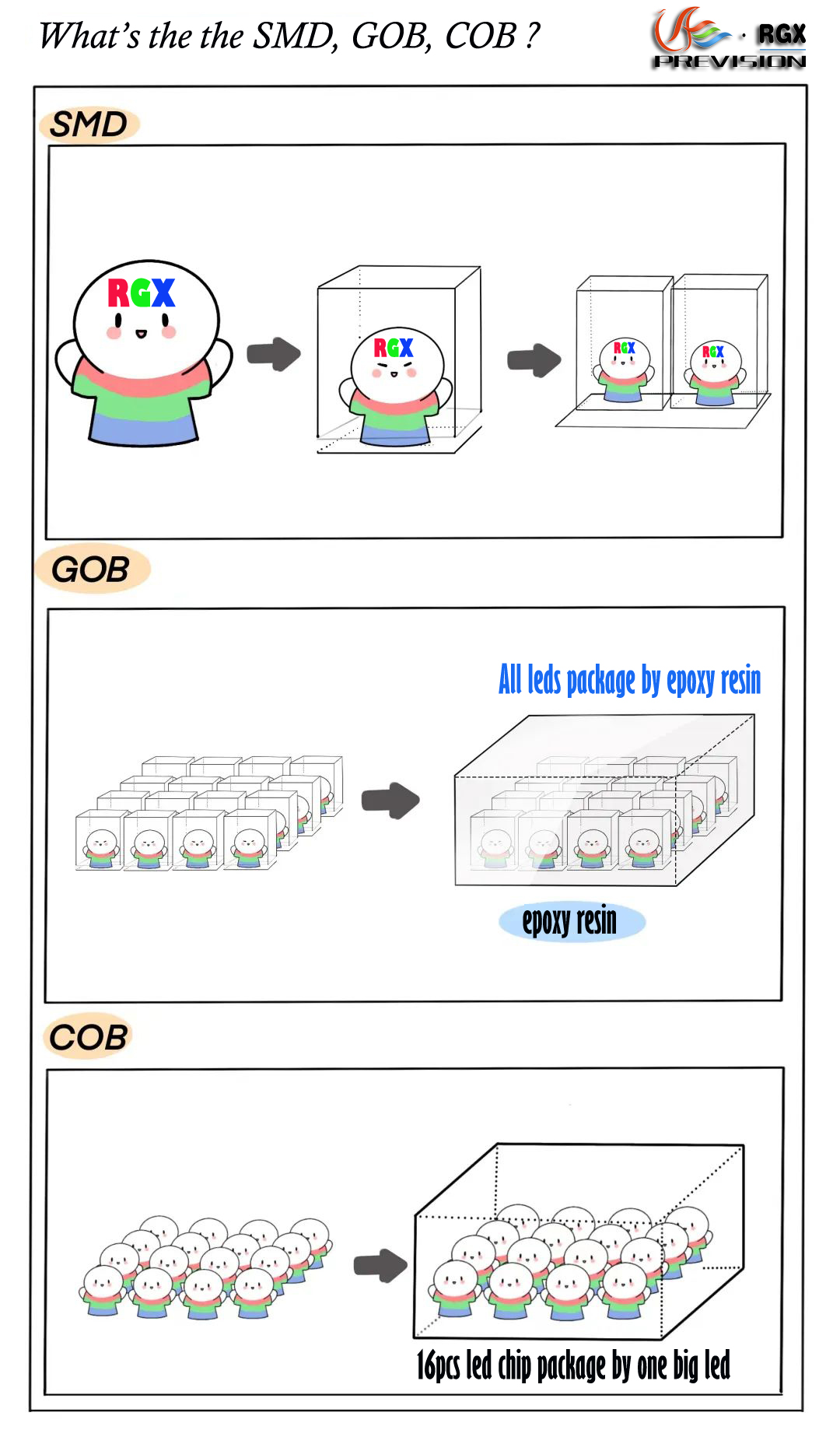
Hello everyone! My name is GOB, which is called Glue on Board. Based on your knowledge of my famous peers SMD and COB, I will direct you to the picture above and let you get the difference and connection between us in 3 seconds as a member of packaging technology.

Simply say, RGX is a technical improvement and extension of the traditional SMD sticker display module technology. In other words, an integral layer of glue is applied to the module surface in the final process after SMT placement and aging, so as to replace the traditional mask technology to upgrade the anti-knock performance of the module.
Q2 Why did you enter the track with micro-spacing below P1.0mm?
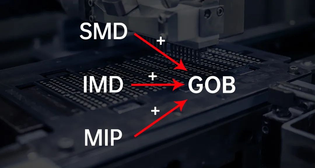
GOB: It's a long story. COB and I both became members of the industry as the same potential players who were expected to break the technical shackles of SMD and expand the space between the dots. During the period of small spacing, I did not get as much attention from the market as COB. The reason was that I had a technical difference with several mainstream players in essence: they were complete and independent packaging systems, while I was an extension of the technology based on the existing technology system. Take the game position as an example, they are playing in the middle field to Carry the whole field, I am more suitable for the auxiliary position, responsible for cooperating with the main force to give skill transfusion and ammunition supplement. After realizing this, I changed my role by virtue of my homologous SMD background, and advanced into micro-spacing with additional attributes. I superposition and match with IMD and MIP, respectively, to add value to the display application of the two point spacing below P1.0mm, innovate the existing micro-spacing display technology pattern, and fully radiate my own light and value.

Q3: Will the entry of GOB break the original scale between IMD and COB?
GOB: With my input of 1+1 > 2, the results of the technical interaction will be quite different. Packaging technology has its strengths, but the market demand determines that we need to develop performance in multiple aspects, so I will compare "IMD+GOB" and "COB" through PK way, so that everyone can measure the level of both comprehensively and fairly. In view of the previous article "5 minutes to take you to understand the differences between IMD and COB packaging technology", IMD has been the absolute advantage of display effect, product yield, manufacturing cost, scale speed and several aspects of IMDvsCOB has won the first victory in the PK. This time, I only singled out my own GOB and COB for the final game.
ROUND 1: Dependability
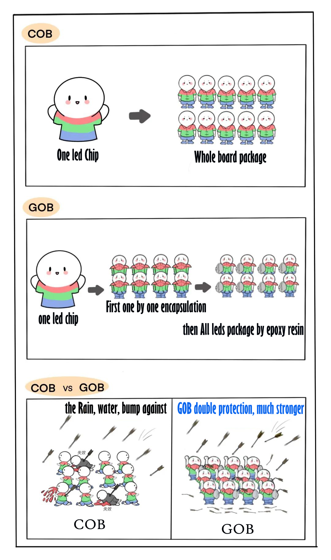
1, human knock, impact: in practical application, the screen body is difficult to avoid the external force of traffic and handling process impact, so anti-knock performance has always been a big consideration for manufacturers. As for the high protection display module technology, I also have high and low protection level with COB. COB is the chip directly welded on the circuit board and then integrated glue; I first encapsulated the chip in the lamp bead, then welded it on the circuit board, and finally integrated glue. Compared with COB more than a layer of encapsulation protection, anti-knock ability is superior.
2. External force of natural environment: Using epoxy resin with ultra-high transparency and ultra-strong thermal conductivity as adhesive material, I can realize real moisture proof, salt spray proof and dust proof to apply to more kinds of harsh environment.

ROUND 2:Display effect
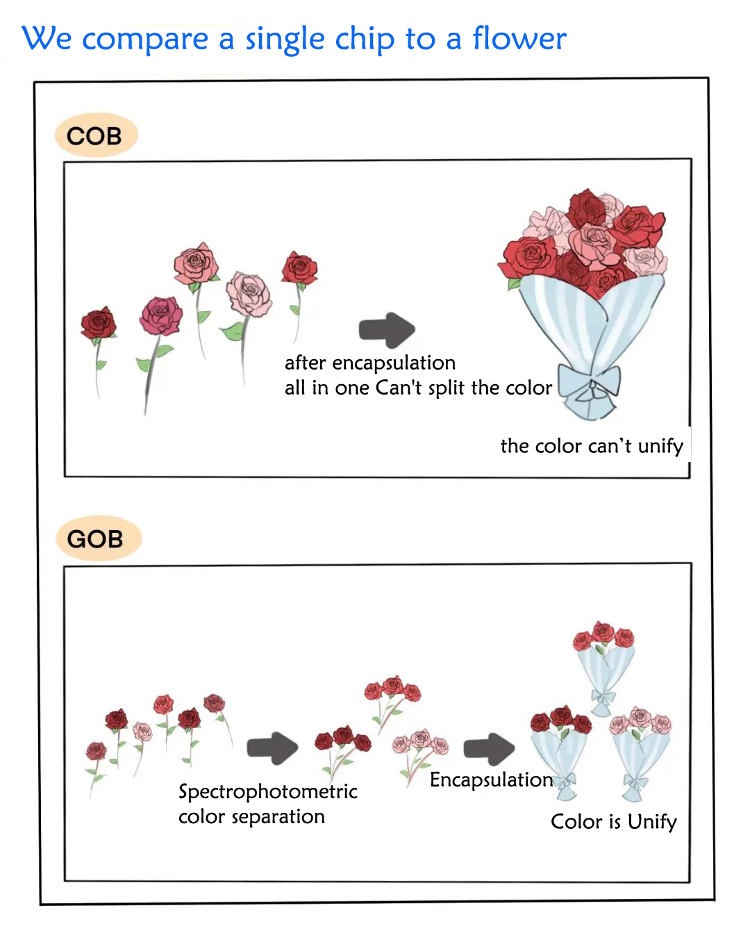
COB’S are risky in the process of separating wavelengths and colors and picking up chips on the board, making it difficult to achieve perfect color uniformity for the entire display. Before the special adhesive, I will manufacture and test the module in the same traditional way as the ordinary module, so as to avoid the bad color difference and Moore pattern in the splitting and color separation, and obtain good color uniformity.

ROUND 3:Cost
With fewer processes and fewer materials required, manufacturing costs are theoretically lower. However, because COB adopts whole board packaging, it must be passed once in production to ensure that there are no bad points before packaging. The smaller the point spacing and the higher the precision, the lower the product yield. It is understood that the current COB normal product shipment rate is less than 70%, which means that the overall manufacturing cost also has to share about 30% of the hidden cost, the actual expenditure is much higher than expected. As an extension of SMD technology, we can inherit most of the original production lines and equipment, with large cost simplification space.